How to use a soldered breadboard? What is a development board

For setting up and testing homemade electronic devices Radio amateurs use so-called breadboards. The use of a breadboard allows you to check, adjust and test the circuit even before the device is assembled on the finished product. printed circuit board.
This allows you to avoid design errors, as well as quickly make changes to the developed circuit and immediately check the result. It is clear that development board, certainly saves a lot of time and is very useful in the ham radio workshop.
The progress and development of electronics also affected breadboards. Currently it is possible without special problems purchase a solderless breadboard. What are the advantages of such a solderless breadboard? The most important advantage of a solderless circuit board is the absence of the soldering process when prototyping the circuit. This circumstance significantly reduces the process of prototyping and debugging of devices. You can assemble a circuit on a solderless circuit board in just a couple of minutes!
How does a solderless breadboard work?
A solderless breadboard consists of a plastic base containing a set of conductive contact connectors. There are a lot of these contact connectors. Depending on the design of the breadboard, the contact connectors are combined into rows, for example, 5 pieces each. The result is a five-pin connector. Each of the connectors allows you to connect leads to it electronic components or current-carrying conductors with a diameter, as a rule, of no more than 0.7 mm.
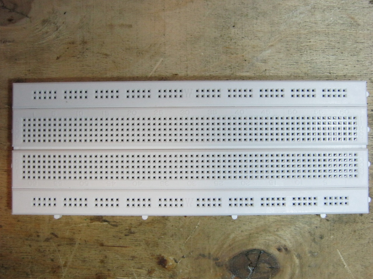
But, as they say, it is better to see once than to hear a hundred times. This is what a solderless breadboard looks like EIC-402 for solderless mounting at 840 points. Thus, this development board contains 840 pin headers!

The base of the breadboard is ABS plastic. The contact connectors are made of phosphor bronze and plated with nickel. Thanks to this, the contact connectors (points) are designed for 50,000 connection/disconnection cycles. Contact connectors allow you to connect leads of radio components and conductors with a diameter of 0.4 to 0.7 mm.
And this is what a development board for Pic series microcontrollers looks like, assembled on a solderless breadboard.


As you can see, a solderless breadboard allows you to install resistors, capacitors, microcircuits, LEDs and indicators. Incredibly simple and convenient.

A solderless breadboard makes learning electronics fun. Circuit diagrams are assembled on a breadboard without any extra effort. Everything is as simple as if you were playing with a LEGO constructor.
Depending on the “steepness” of a solderless breadboard, it can be equipped with a set of connecting conductors (jumper wires), additional connectors, etc. Despite all the “goodies,” the main indicator of the quality of a solderless breadboard is still the quality of the contact connectors and their quantity. Everything is clear here, the more contact points (connectors), the more complex the circuit can be mounted on such a board. The quality of the connectors is also important, because from frequent use the connectors can lose their elastic properties, and this will lead to poor quality contact.
Since the breadboard connectors allow you to connect conductors with a diameter of no more than 0.4-0.7 mm, attempts to “push” thick pins of parts can only lead to damage to the contact. In this case, it is better to solder or wind a wire of a smaller diameter to the terminals of radio elements that have a fairly large diameter, for example, like those of powerful diodes, and only then connect the element to the breadboard.
If you plan to design enough complex circuit With a large number elements, then the solderless breadboard area may not be enough. In this case, it is better to divide the circuit into blocks, each of which must be assembled on a separate breadboard and then connect the blocks into a single device using connecting conductors. It is clear that in this case an additional development board will be needed.
As a rule, a breadboard with a set of connecting conductors of different lengths (jumper wires) is more expensive than conventional solderless boards, which are not equipped with such conductors. But it doesn't matter. Ordinary insulated wire can also be used as connecting conductors.
For example, a very common and affordable wire is perfect for such purposes VSWR 4x0.4, which is used for installation of security and fire alarm systems. This wire has 4 cores, each of which is covered with insulation. The diameter of the copper core itself, excluding insulation, is 0.4 mm. The insulation from such a wire can be easily removed with wire cutters, and the copper wire is not coated with varnish.
From one meter of such cable you can make a whole lot of connecting conductors of different lengths. By the way, in the photographs of the breadboard shown above, the KSVV wire was used to connect the radio components.
The breadboard should be protected from dust. If the layout for a long time is not used, then dust settles on its surface, which clogs the contact connectors. In the future, this will lead to poor contact and the breadboard will have to be cleaned.
Solderless breadboards are not designed to work with 220 volts! It is also worth understanding that prototyping and testing work high current circuits on a solderless breadboard may cause overheating of the pin connectors.
Shielding a breadboard.
Preparing a solderless breadboard before work.
Before you start prototyping the circuit on a new solderless breadboard, it would be a good idea to “ring” the contact connectors with a multimeter. This is necessary in order to find out which connector points are connected to each other.
The fact is that the points (connectors) on the breadboard are connected on the breadboard in a special way. For example, the solderless breadboard EIC-402 has 4 independent contact zones. The two on the edges are power buses (positive " + " and minus " - "), they are marked with a red and blue line along the contact points. All points of the bus are electrically connected to each other and essentially represent one conductor but with a bunch of connector points.

The central area is divided into two parts. In the middle, these two parts are separated by a kind of groove. Each part has 64 lines with 5 connector points each. These 5 connector points in the row are electrically connected to each other. Thus, if you install, for example, a microcircuit in a DIP-8 or DIP-18 package in the center of the breadboard, then to each of its pins you can connect either 4 pins of radio elements or 4 connecting conductors-jumpers.

Also, power rails on both sides of the breadboard will remain available for connection. It is quite difficult to explain this in words. Of course, it’s better to see it live and play enough with solderless development board. This is the circuit I assembled on a solderless board. This is the simplest development board for PIC series microcontrollers. It is equipped with a PIC16F84 microcontroller and hardware elements: indicator, buttons, buzzer...

The solderless development board is convenient to use for quick assembly measuring circuits, for example, to test the IR receiver.
Such boards can be purchased not only on radio markets, but also bought on the Internet.
Cheap solderless breadboards can be purchased on AliExpress.com. I talked about how to buy radio parts and kits on AliExpress.
Making a printed circuit board at home is so easy that it’s even funny to talk about. Just print on laser printer a picture with conductors, and then press it onto the blank of the future board with an iron. All that remains is to soak the paper with water and etch the board in the etching solution.
The technology is so good and, one might say, lazy that even when only one copy is made, a printed circuit board is made. Although printed circuit boards do not have any advantages compared to surface-mounted installations, unless the production of several copies of the same device is required.
But, before assembling a printed circuit board, the circuit is most often assembled on a breadboard. In the simplest case, on a piece of textolite, plywood or thick cardboard, power buses made of tinned wire with a diameter of at least 1 mm are fixed at the edges so that the mechanical strength of the installation is sufficient. Everything that should be connected to them is soldered to the power buses, and the remaining connections are made through the leads of the parts.
Collect one breadboard diagram this is a whole art. Some specialists were able to assemble on such a board circuits of twenty or more microcircuit packages in DIP-14 type packages. In this case, pins 7 and 14 are soldered to the power buses, or as they now say in a foreign manner, pins (from English pin) 7 and 14, and all the remaining connections are made with insulated mounting wire of a suitable diameter. In addition to the power buses, you can install additional pads in the form of pieces of wire inserted into the holes of the board.
But such layout methods sometimes led to disastrous results. As a result of numerous re-solderings, the leads of the parts simply burned out and fell off. Such parts were simply unsuitable for further use. Such situations can be avoided by modern solderless breadboards. What is it and what is it eaten with? Let's try to figure this out.
Solderless breadboards- This is an indispensable thing for experiments with electronic equipment. In English it is called breadboard, which translates as a breadboard for ease of experimentation, breadboard electronic circuit(dictionary "Multitran"). One such board is shown in Figure 1.
Figure 1. Basic solderless breadboard.
When developing electronic circuits, you often have to follow the path of trial and error. Even if the circuit is not our own design, but simply a repetition of someone else’s design, sometimes selection of modes of transistors and microcircuits is required. Assembled circuit requires frequent replacement of parts, which, you see, with repeated soldering can lead to consequences, if not tragic, then, in any case, difficult to correct.
Homemade breadboards. Is it possible to save money on them?
Some enthusiasts still propose making solderless breadboards using a makeshift method. Similar descriptions can be found on the Internet. The materials for such homemade boards are textolite, tin from cans and rivets.
Moreover, all this is done manually or, as they often say, on the knee: tin is cut into strips and bent in a certain way. After which, again manually, the textolite plate is marked and holes are drilled in it. Then homemade contacts are riveted. (On branded breadboards, the contacts are made of springy metals, which will be discussed below.) The reliability and durability of such a design will not be the highest.
Again, as in some other cases, the time of one’s own work is not taken into account. And at the same time, if you go at least to online stores, you can make sure that the cost of development boards is not too high. For example, the cost of the board shown in Figure 1 is about 10 dollars, or about 300-odd rubles.
Of course, there are fees and large sizes, and naturally their cost increases. When purchasing development boards on e-bay or Aliexpress, the price may be even lower.
What types of breadboards are there and how are they designed?
The solderless breadboard consists of a plastic base with square holes at 2.54 mm or 0.1 inch pitch on the top side. This is precisely the step taken by the conclusions of imported microcircuits. This quantity in English-speaking countries has its own name: line line, in in this case measure of length.
Domestic microcircuits have a pin pitch of exactly 2.5 mm, because we have a metric system. If the microcircuit body is not very long, then such a discrepancy is practically not noticeable. It is easy to calculate that for ten pins there will be a difference of 0.4 mm, and if the microcircuit has 40 legs (twenty on each side) then the discrepancy is already 0.8 mm, the pins have to be moved apart somewhat. True, domestic microcircuits in such large packages are currently not used at all.
Figure 2 shows another prototype board option. It is not much different from the board shown in Figure 1, except for the numbering of the holes with letters and numbers. This is quite convenient: if on the circuit diagram near the rations you mark with a pencil their positions on the breadboard, then in the future it will be much easier to figure out where everything comes from. (Sometimes it happens that a half-assembled circuit lies for quite a long time, and what was done before is simply forgotten.)

Figure 2. Solderless breadboard
Between the power buses there are holes, also grouped in groups of 5. Their connection inside the board is shown in Figure 3.

Figure 3. Solderless breadboard design
And Figure 4 shows the design of the contacts.

Figure 4. Solderless breadboard pin design
There are latches on the sides of the breadboards that allow you to produce larger boards. Such a board is shown in Figure 5.

Figure 5. Large size solderless breadboard
On the bottom surface of the board there is double-sided tape covered with wax paper. If you peel off this paper, then ready-made board can be attached inside any structure. This is quite acceptable if you simply don’t have enough time to design and solder a real printed circuit board.
The reliability of branded solderless boards is quite high, as can be judged by the product label shown in Figure 6.

Figure 6. Product label on solderless breadboard
Of course, everything is written in English, but you can roughly figure it out. The most top line suggests that this is a solderless breadboard with square holes in an ABS plastic case, released by Chinese company EIC. On the surface of the board there is a color print indicating the power lines and hole numbering.
The board is designed to operate at temperatures up to 84 o C. The contacts are made of phosphor bronze (it has good springing properties) and coated with a layer of nickel. The durability of the contacts is 50,000 connections, which is quite enough for several years of operation. The diameter of the parts and conductors inserted into the holes of the leads is in the range of 0.4...0.7 mm. (Remember homemade contacts made from tin cans).
The number of holes on the board is 400, board dimensions are 84*54 mm. Board model EIC-801. To increase the size, the board allows you to attach additional boards.
Figure 7 shows a circuit assembled on a breadboard using chips in DIP packages.

Figure 7. Circuit on breadboard
Connecting wires from old TVs
Connecting wires are also sold with the boards, sometimes as kits. For some reason, the price of such wires is quite high, so you can simply use pieces of mounting wire of a suitable diameter or make such wires yourself.
The easiest way for these purposes is to use a flat cable from TVs of the 3USTST series. Remember, there were pin contacts coming out of plastic cases? Such televisions have long been thrown into landfills as morally and physically obsolete. Such a loop is shown in Figure 8.

Figure 8. Loop from old radio equipment
The connector shown in the photo should be disassembled into separate wires, the same contacts should also be soldered onto the reverse ends, and. Everyone probably imagines this process, so there is no need to describe it here.
That seems to be all that can be said about the use of solderless breadboards. But there will be a very attentive reader who will exclaim: “Excuse me, why isn’t a word said about prototyping circuits on SMD chips?” and, perhaps, he will be right. After all, it is they, with their numerous thin and not very strong conclusions, that will first of all become victims of experiments with electricity.
For prototyping with this type of component, you should use adapter boards that convert SMD-mounted housings into DIP housings. Some adapter boards are shown in Figures 9 - 10.

Figure 9.

Figure 10.
In the next article I will share some secrets for using solderless breadboards.
All people in the world, young and old, know that before you create anything, you must first create a model of this “something,” be it a model of a building, a stadium, or even a small rural toilet. In electrical engineering this is called a prototype. A prototype is a working model of a device. Therefore, experienced electronics engineers, before assembling a device according to a circuit on the Internet, posted by no one knows who and no one understands why, must make sure that this circuit will actually work. Therefore, the circuit needs to be quickly assembled and made sure it works, that is, assembled layout. Well, in order to assemble it, that’s exactly what we need breadboard.
Types of development boards
Thick cardboard
A long time ago, when you were not even in the plans, our grandfathers, and maybe grandmothers, you never know :-), used thick cardboard. This is the fastest and cheapest way to test circuits. Holes were cut in the cardboard for the terminals of the radio elements and on the other side they were connected using wires and other elements if they did not fit on the front side. It looked something like this:
A is the front side, B is the back side.
Everything would be fine, but I had to solder the conclusions, make sure that nothing short-circuited anywhere, and while you are “sculpting” this circuit, you can even inadvertently get confused :-). Yes, and somehow it’s not beautiful.
Homemade breadboards
I still found these times at the radio circle. Back then we made breadboards ourselves. We took a sharp cutter and cut squares on foil PCB. Next, they were covered with solder.
If we needed to connect tracks somewhere, we simply made jumpers between the squares with a drop of solder. It turned out high quality and beautiful. If you were too lazy to solder the radio elements onto a normally wired board with tracks, you simply left it as is and used the device.
Disposable development boards
Manufacturers still “fucked up” on this matter, or as they say in economics, demand creates supply. Ready-made mock-up scarves, single-sided and even double-sided, began to appear for every size and taste.


By the way, you can find them on Ali right away a whole set .
The holes are very conveniently matched to the sizes of the pins of the microcircuits, as well as other radio elements. Therefore, it is very convenient to assemble and test electronic devices on such breadboards. Yes, and they are inexpensive.

Reverse side Such development boards with ready-made devices will look something like this:

What are the disadvantages of these development boards? It is still better to use them once, since with repeated use their spots may fly off, which will lead to its unsuitability.
Solderless breadboards
Progress is moving with its confident steps across our world, and now they have appeared on the market solderless breadboards.
They cost a little more than simple disposable breadboards, but honestly, it's worth it.
They are very convenient in terms of installing parts, as well as their connection with each other. Wires no larger than 0.7 mm and no less than 0.4 mm in diameter can be inserted into such breadboards. To find out which holes and tracks communicate with each other, we check the whole thing. For design large circuits(suddenly you will develop some kind of control unit for a hadron collider) you can add the same breadboards back to back. There are special ears for this. One move, and the breadboard will become a little larger.


Well, what kind of breadboard can there be without connecting wires? Connecting wires or jumpers ( from English- jump), are needed to connect radio components on the breadboard itself.

A little later I bought these jumpers from Aliexpress. They are much more convenient than wire ones:
.JPG)
Everything is simple here, take the jumper and insert it with a slight movement of the hand


Let's put together a simple circuit for turning on an LED via a button on a breadboard

This is what she will look like

Set the Power Supply to 5 Volts and press the button. The LED lights up bright green. This means that the scheme is workable, and we can use it at our discretion.

Conclusion
Solderless breadboards are taking the world by storm. Any circuit on them can be assembled and disassembled in a matter of minutes. After assembling and checking the circuit on the breadboard, you can safely begin assembling it in its pure form. I think every self-respecting electronics engineer should have such a breadboard. But keep in mind that it is better not to test circuits with a large current in the circuit, since the contacts of the prototype boards can simply burn out - Joule-Lenz law. Good luck in the development and construction of radio-electronic devices!
Where to buy a development board
A breadboard with flexible jumpers and even a ready-made 5 Volt power supply can be immediately purchased as a kit on Aliexpress. Choose to your taste and color!

If you don’t want to, then the easiest way would be to buy a disposable breadboard and assemble a finished device on it:
Often, in order to quickly assemble a prototype of some electronic circuit on the table, it is convenient to use a breadboard, which allows you to do without soldering. And only then, when you are convinced that your circuit is working, can you bother creating a printed circuit board with soldering. For a person just starting to explore the world of electronics, it may not be at all obvious to use a tool such as a breadboard or breadboard. Let's see what a development board is and how to work with it.
Instructions for working with a solderless breadboard (breedboard)
We will need:
- Breadboard, buy;
- connecting wires (I recommend this set);
- LED (can be purchased);
- a resistor with a resistance of 330 Ohms or close to it (an excellent set of resistors of all popular values);
- 9 volt Krona battery.
1 Description breadboard
There are many types of breadboards. They differ in the number of pins, number of buses, and configuration. But they are all arranged according to the same principle. A development board consists of a plastic base with many holes, usually spaced at a standard 2.54mm pitch. The legs of the output microcircuits are usually located with the same pitch. The holes are needed to insert the leads of radio elements or connecting wires into them. A typical view of a breadboard is shown in the figure.
Various types of breadboards
This type of board received its English name - breadboard ("board for bread") due to comparison with a board for slicing bread: it is suitable for quickly "cooking" simple circuits.
There are also breadboards for soldering. They differ in that they are usually made of fiberglass, and their metallized pads are well suited for soldering wires and lead radio elements to them. In this article we do not consider such boards.
2 Device breadboard
Let's see what's inside the breadboard. The picture on the left shows general view fees. On the right side of the figure, the conductor buses are indicated in color. Blue- this is the “minus” of the circuit, red is “plus”, green are conductors that you can use at your discretion to connect parts electrical diagram, assembled on a breadboard. Note that the center holes are connected in parallel rows across the breadboard, not lengthwise. Unlike the power rails, which are located along the edge of the breadboard along its edges. As you can see, there are two pairs of power rails, which allows you to supply two different voltages to the board if necessary, for example, 5 V and 3.3 V.
 Breadboard device
 The two groups of transverse conductors are separated by a wide groove. Thanks to this recess, microcircuits in DIP packages (cases with “legs”) can be placed on the breadboard. Like the picture below:

There are also radioelements for surface mounting (their “legs” during installation are not inserted into holes in the printed circuit board, but are soldered directly to its surface). They can be used with such a breadboard only with special adapters - clamping or soldering. Universal adapters are called “zero gain panels” or ZIF panels, using foreign terminology. Such adapters are most often for 8-pin microcircuits and for 16-pin microcircuits. An example of such elements and such an adapter is shown in the illustration.

The numbers and letters on the breadboard are needed so that you can more easily navigate the board, and, if necessary, draw and sign your schematic diagram. This can sometimes be useful when installing large circuits, especially if you are installing according to the description. Use them in much the same way as letters and numbers on a chessboard, for example: connect the resistor output to socket E-11, etc.
3 Assembling the circuit on a breadboard
To acquire the skill of working with a breadboard, we will assemble the simplest scheme as shown in the picture. We connect the “plus” of the battery to the positive bus of the breadboard, the “minus” - to the negative bus. The bright red and black lines are the connecting wires, and the pale translucent ones are the connections provided by the breadboard, they are shown for clarity.
When circuits are soldered, you can do everything without additions. But then there is a fairly high probability that something may short-circuit. And then the scheme will not work. To eliminate this drawback and bring the results of the work into a more or less decent form, they use such a simple and effective invention as a breadboard. What is she? What varieties are there?
Development board
How to use such an invention? First, let's clarify the terminological component. A development board is a universal blank that is used to assemble and simulate prototypes of electronic devices. They can be divided into two types:
- Those where soldering is used.
- Those where there is no soldering.
When creating prototypes of electronic devices, everyone faces several problems:
- The breadboard must be designed from scratch and then manufactured. If an error is made, it will have to be redone.
- Creating a single copy is usually not profitable.
- If the circuit is made on microcircuits with a low degree of integration and analog elements, then it will be easier to make it using wall-mounted installation. But it will be very difficult to make microprocessor devices in this way.
Beginning radio amateurs are in the least advantageous position: since they do not yet have the skills to design circuits, they have to operate “at random.” Therefore on at the moment A wide range of different breadboards are produced, where different short tracks are laid, and a person will only have to connect the parts to get the necessary circuit.
Varieties

There are several types of breadboards:
- Universal. They only have metallized holes that will be connected by the developer.
- For digital devices. There are separate places in them where microcircuits can be placed. There are also power supply buses throughout the board.
- Specialized. Created for various devices, which must work on certain chips. As a rule, they are very functional and well-designed.
Also, depending on how they are made, there are two types:
- Solderless breadboard. The advantages of this type are usually called integrity and accuracy of execution (if we talk about industrial designs).
- Soldered breadboard. Cheapness and opportunity easy change devices - these are the main advantages of this type.
Development boards for socket mounting

Such blanks have thousands of holes that are connected to each other by means of metal strips. The leads of microcircuits and radio components are inserted into the holes and then connected using jumpers. The long rows of pins that can be seen at the bottom, middle, and top of the board are the power rails. They are used to connect multiple points in a circuit to ground and the power supply. Under each hole there is an elastic contact special form, which ensures high conductivity and durability of connections. The development board is stackable. In such cases, grooves are located on the side faces to connect several devices into one large one.
Conclusion
The development board significantly simplifies the developer’s work. It also increases the stability of the circuit, so don’t hesitate to use the device. It should also be noted important role, which a development board plays for people just starting to develop electronic devices, because many of these blanks are already produced for the creation of certain devices. Therefore, when designing a popular circuit, it makes sense to look to see if there is already a blank for it, because if the answer is positive, then this will significantly save time.