What is the active mode of a transistor. What is a bipolar transistor and how to test it
Bipolar transistors These are semiconductor devices with three electrodes connected to three layers in series, with different conductivities. Unlike other transistors, which carry one type of charge, it is capable of carrying two types at once.
Connection diagrams using bipolar transistors depend on the work performed and the type of conduction. Conduction can be electronic or hole.
Types of bipolar transistors
Bipolar transistors are divided according to various criteria into types according to:
- Material of manufacture: silicon or gallium arsenide.
- Frequency value: up to 3 MHz – low, up to 30 MHz – medium, up to 300 MHz – high, more than 300 MHz – ultra-high.
- Highest power dissipation: 0-0.3 W, 0.3-3 W, over 3 W.
- Device type: 3 layers of semiconductor with sequential order of conduction type.
Design and operation
The transistor layers, both inner and outer, are combined with built-in electrodes, which are named base, emitter and collector.
There are no significant differences in the types of conductivity between the collector and emitter, however, the percentage of inclusion of impurities in the collector is much lower, which makes it possible to increase the permissible voltage at the output.
The middle layer of the semiconductor (base) has a high resistance value, since it is made of lightly doped material. It is in contact with the collector over a large area. This makes it possible to increase heat dissipation, which is necessary due to the release of heat from the displacement of the junction in the other direction. Good contact base with a collector allows electrons, which are minority carriers, to easily pass through.
The transition layers are made according to the same principle. However, bipolar transistors are considered as unbalanced devices. When alternating the outer layers in places with the same conductivity, it is impossible to form similar semiconductor parameters.
The transistor connection circuits are designed in such a way that they can provide it with both a closed and an open state. At active work When the semiconductor is open, the emitter bias is in the forward direction. To fully understand this design, you need to connect the supply voltage according to the diagram shown.

In this case, the boundary at the 2nd junction of the collector is closed, no current flows through it. In practice, the opposite phenomenon occurs due to adjacent transitions and their influence on each other. Since the minus pole of the battery is connected to the emitter, the open-type transition allows electrons to pass to the base, where they recombine with holes, which are the main carriers. Base current I b appears. The higher the base current, the higher the output current. This is the principle of operation of amplifiers.
Only diffusion movement of electrons occurs through the base, since there is no electric field work. Due to the small thickness of this layer and a significant gradient of particles, almost all of them enter the collector, although the base has high resistance. At the junction there is an electric field that promotes the transfer and draws them in. The emitter and collector currents are the same, except for a small loss of charge from redistribution at the base: I e = I b + I k.
Characteristics
- Current gain β = I k / I b.
- Voltage Gain U eq / U be.
- Input resistance.
- Frequency characteristic is the ability of a transistor to operate up to a certain frequency, beyond which the transition processes lag behind the change in the signal.
Operating modes and schemes
The type of circuit affects the mode of operation of the bipolar transistor. The signal can be received and transmitted in two places for different cases, and there are three electrodes. Consequently, one arbitrary electrode must be both an output and an input. All bipolar transistors are connected according to this principle, and they have three types of circuits, which we will consider below.
Common collector circuit
The signal passes through the resistance R L, which is also included in the collector circuit.

This connection diagram makes it possible to create just a current amplifier. The advantage of such an emitter follower is the formation of significant resistance at the input. This makes it possible to match the amplification stages.
Scheme with a common base

The circuit has a drawback in the form of low input resistance. A common base circuit is most often used as an oscillator.
Scheme with common emitter
Most often, when using bipolar transistors, a circuit with a common emitter is used. The voltage passes through the load resistance R L, and the power is connected to the emitter with the negative pole.

Signal variable value comes to the base and emitter. In the collector circuit it becomes larger in value. The main elements of the circuit are a resistor, a transistor and an amplifier output circuit with a power supply. Additional steel elements: container C 1, which prevents current from passing to the input, resistance R 1, thanks to which the transistor opens.
In the collector circuit, the transistor voltage and resistance are equal to the EMF value: E= Ik Rk +Vke.
It follows that the small signal Ec determines the rule for changing the potential difference into the variable output of the transistor converter. This circuit makes it possible to increase the input current many times, as well as voltage and power.
One of the disadvantages of such a circuit is the low input resistance (up to 1 kOhm). As a consequence, problems arise in the formation of cascades. The output resistance is from 2 to 20 kOhm.
The considered circuits show the action of a bipolar transistor. Its operation is affected by signal frequency and overheating. To resolve this issue, additional separate measures are applied. Emitter grounding produces distortion at the output. To create the reliability of the circuit, connect filters, feedback etc. After such measures, the circuit works better, but the gain decreases.
Operating modes
The speed of the transistor is influenced by the magnitude of the connected voltage. Let's consider different modes work on the example of a circuit in which bipolar transistors are connected to a common emitter.
Cutoff
This mode is formed when the voltage V BE decreases to 0.7 volts. In this case, the emitter junction closes and there is no current at the collector, since there are no electrons in the base, and the transistor remains closed.
Active mode
When a voltage sufficient to turn on the transistor is applied to the base, a small input current and a large output current occur. This depends on the size of the gain. In this case, the transistor works as an amplifier.
Saturation mode
This work has its differences from the active mode. The semiconductor opens completely, the collector current reaches highest value. Its increase can be achieved only by changing the load or the EMF of the output circuit. When adjusting the base current, the collector current does not change. The saturation mode has the peculiarities that the transistor is fully open and operates as a switch. If you combine the saturation and cutoff modes of bipolar transistors, you can create switches.
The properties of the output characteristics affect the modes. This is shown in the graph.

When plotting segments corresponding to the highest collector current and voltage size on the coordinate axes, and then connecting the ends with each other, a red load line is formed. The graph shows that the point of current and voltage will move upward along the load line as the base current increases.
The area between the shaded output characteristic and the Vke axis is the cutoff work. In this case, the transistor is closed, and the reverse current is small. The characteristic at point A at the top intersects with the load, after which with a subsequent increase in I B the collector current no longer changes. On the graph, the saturation area is the shaded part between the Ik axis and the steepest graph.
Bipolar transistors in various modes
Transistor interacts with signals different types in input circuit. The transistor is mainly used in amplifiers. The input AC signal changes the output current. In this case, circuits with a common emitter or collector are used. The output circuit requires a load for the signal.
Most often, a resistance installed in the collector output circuit is used for this. With him making the right choice, the output voltage will be much greater than the input.
During pulse signal conversion, the mode remains the same as for sinusoidal signals. The quality of the harmonic change is determined by the frequency characteristics of the semiconductors.
Switching mode
Transistor switches are used for contactless switching in electrical circuits. This work consists of intermittently adjusting the resistance value of the semiconductor. Bipolar transistors are most used in switching devices.
Semiconductors are used in signal modification circuits. Their universal work and a broad classification makes it possible to use transistors in various circuits, which determine their operating capabilities. The main circuits used are amplifying and switching circuits.
Good afternoon, friends!
Today we will continue to get acquainted with the electronic “building blocks” of computer hardware. We have already looked at how they work field effect transistors, which are necessarily present on every motherboard computer.
Sit back comfortably - now we will make an intellectual effort and try to figure out how it works
Bipolar transistor
A bipolar transistor is semiconductor device, which is widely used in electronic products, including computer units nutrition.
The word “transistor” is derived from two English words – “translate” and “resistor”, which means “resistance converter”.
The word “bipolar” means that the current in the device is caused by charged particles of two polarities – negative (electrons) and positive (so-called “holes”).
“Hole” is not jargon, but a completely scientific term. A “hole” is an uncompensated positive charge or, in other words, the absence of an electron in the crystal lattice of a semiconductor.
![]() A bipolar transistor is a three-layer structure with alternating types of semiconductors.
A bipolar transistor is a three-layer structure with alternating types of semiconductors.
Since there are two types of semiconductors, positive (positive, p-type) and negative (negative, n-type), there can be two types of such a structure - p-n-p and n-p-n.
The middle region of such a structure is called the base, and the outer regions are called the emitter and collector.
In the diagrams, bipolar transistors are designated in a certain way (see figure). We see that the transistor is, essentially, yes p-n junction, connected in series.
A quick question: why can’t the transistor be replaced with two diodes? After all, each of them has a p-n junction, right? I connected two diodes in series - and it was done!
No! The fact is that the base in the transistor is made very thin during manufacturing, which cannot be achieved by connecting two separate diodes.
The principle of operation of a bipolar transistor
The basic principle of operation of a transistor is that it does not high current The base can control a much larger collector current - in the range from almost zero to a certain maximum possible value.![]() The ratio of the collector current to the base current is called the current gain and can range from several units to several hundred.
The ratio of the collector current to the base current is called the current gain and can range from several units to several hundred.
It is interesting to note that for low-power transistors it is most often greater than for high-power ones (and not vice versa, as one might think).
The difference is that, unlike the PT gate, during control the base current is always present, i.e. Some power is always spent on control.
The greater the voltage between the emitter and the base, the greater the base current and, accordingly, the greater the collector current. However, any transistor has maximum permissible voltage values between the emitter and base and between the emitter and collector. If you exceed these parameters, you will have to pay with a new transistor.
In operating mode, usually the base-emitter junction is open and the base-collector junction is closed.
![]() A bipolar transistor, like a relay, can also operate in switching mode. If you apply some sufficient current to the base (close button S1), the transistor will be well open. The lamp will light up.
A bipolar transistor, like a relay, can also operate in switching mode. If you apply some sufficient current to the base (close button S1), the transistor will be well open. The lamp will light up.
In this case, the resistance between the emitter and collector will be small.
The voltage drop across the emitter-collector section will be several tenths of a volt.
If you then stop supplying current to the base (open S1), the transistor will close, i.e. the resistance between the emitter and collector will become very large.
The lamp will go out.
How to test a bipolar transistor?
![]() Since a bipolar transistor consists of two pn junctions, checking it with a digital tester is quite simple.
Since a bipolar transistor consists of two pn junctions, checking it with a digital tester is quite simple.
It is necessary to set the tester operation switch to position, connecting one probe to the base, and the second – alternately to the emitter and collector.
Essentially, we just check sequentially p-n serviceability transitions.
Such a transition can be either open or closed.
 Then you need to change the polarity of the probes and repeat the measurements.
In one case, the tester will show a voltage drop at the emitter-base and collector-base junctions of 0.6 - 0.7 V (both junctions are open).
In the second case, both transitions will be closed, and the tester will record this.
It should be noted that in operating mode, most often one of the transitions of the transistor is open and the second is closed.
Measuring the current gain of a bipolar transistor
 If the tester has the ability to measure the current transfer coefficient, then you can check the operation of the transistor by installing the transistor leads into the corresponding sockets.
Current transfer coefficient is the ratio of the collector current to the base current.
The higher the gain, the more collector current can be controlled by the base current, all other things being equal.
The pinout (pin name) and other data can be taken from the data sheets (reference data) for the corresponding transistor. Data sheets can be found on the Internet through search engines.
 The tester will show on the display the current transfer (gain) coefficient, which must be compared with the reference data.
The current transfer coefficient of low-power transistors can reach several hundred.
For powerful transistors it is significantly smaller - several units or tens.
However, there are powerful transistors with a transmission coefficient of several hundred or thousand. These are the so-called Darlington pairs.
 A Darlington pair consists of two transistors. The output current of the first transistor is the input current for the second.
The overall current transfer coefficient is the product of the coefficients of the first and second transistors.
The Darlington pair is made in a common housing, but it can also be made from two separate transistors.
Built-in diode protection
![]() Some transistors (power and high voltage) can be protected from reverse voltage built-in diode.
Some transistors (power and high voltage) can be protected from reverse voltage built-in diode.
Thus, if you connect the tester probes to the emitter and collector in diode testing mode, it will show the same 0.6 - 0.7 V (if the diode is forward biased) or a “blocked diode” (if the diode is reverse biased) .
If the tester shows some small voltage, and in both directions, then The transistor is definitely broken and needs to be replaced. A short can also be determined in resistance measurement mode - the tester will show low resistance.
 There is (fortunately, quite rarely) a “mean” malfunction of transistors. This is when it works at first, but after some time (or after warming up) it changes its parameters or fails altogether.
If you unsolder such a transistor and check it with a tester, it will have time to cool before the probes are connected, and the tester will show that it is normal. The best way to verify this is by replacing the “suspicious” transistor in the device.
In conclusion, let’s say that the bipolar transistor is one of the main “pieces of hardware” in electronics. It would be nice to learn to find out whether these “pieces of iron” are “alive” or not. Of course, I have given you, dear readers, a very simplified picture.
In fact, the operation of a bipolar transistor is described by many formulas, there are many varieties of them, but it is a complex science. For those wishing to dig deeper, I can recommend the wonderful book by Horowitz and Hill, “The Art of Circuit Design.”
Transistors for your experiments can be purchased
See you on the blog!
Transistor
Transistor is a semiconductor device that allows weak signal control a stronger signal. Because of this property, they often talk about the ability of a transistor to amplify a signal. Although in fact, it does not enhance anything, but simply allows you to turn on and off a large current with much weaker currents. Transistors are very common in electronics, because the output of any controller can rarely produce a current of more than 40 mA, therefore, even 2-3 low-power LEDs cannot be powered directly from the microcontroller. This is where transistors come to the rescue. The article discusses the main types of transistors, the differences between P-N-P and N-P-N bipolar transistors, P-channel from N-channel field-effect transistors, the main subtleties of connecting transistors are considered and the scope of their application is revealed.
Do not confuse a transistor with a relay. A relay is a simple switch. The essence of its work is to close and open metal contacts. The transistor is more complex and its operation is based on an electron-hole transition. If you are interested in learning more about this, you can watch an excellent video that describes the operation of a transistor from simple to complex. Don’t be confused by the year the video was produced - the laws of physics have not changed since then, and a newer video that presents the material so well could not be found:
Types of transistors
Bipolar transistor
The bipolar transistor is designed to control weak loads (for example, low-power motors and servos). It always has three outputs:
- Base - current is supplied or turned off to open or close the transistor
Collector - served high voltage, which the transistor controls
Emitter (English: emitter) - “output” output of a transistor. Current flows through it from the collector and base.
The bipolar transistor is controlled by current. The more current supplied to the base, the more current will flow from the collector to the emitter. The ratio of the current passing from the emitter to the collector to the current at the base of the transistor is called the gain. Denoted as hfe (in English literature it is called gain).
For example, if hfe= 150, and 0.2 mA passes through the base, then the transistor will pass a maximum of 30 mA through itself. If a component that draws 25 mA (such as an LED) is connected, 25 mA will be provided to it. If a component that draws 150 mA is connected, it will only be provided with the maximum 30 mA. The documentation for the contact indicates the maximum permissible values of currents and voltages base-> emitter And collector -> emitter . Exceeding these values leads to overheating and failure of the transistor.
Funny pictures:
![]()
NPN and PNP bipolar transistors
There are 2 types of polar transistors: NPN And PNP. They differ in the alternation of layers. N (from negative) is a layer with an excess of negative charge carriers (electrons), P (from positive) is a layer with an excess of positive charge carriers (holes). More information about electrons and holes is described in the video above.
The behavior of transistors depends on the alternation of layers. The animation above shows NPN transistor. IN PNP transistor control is the other way around - current flows through the transistor when the base is grounded and is blocked when current is passed through the base. As shown in the diagram PNP And NPN differ in the direction of the arrow. The arrow always points to the transition from N To P:

Designation of NPN (left) and PNP (right) transistors in the diagram
NPN transistors are more common in electronics because they are more efficient.
Field effect transistor
Field effect transistors differ from bipolar ones internal device. MOS transistors are the most common in amateur electronics. MOS is an acronym for metal-oxide-conductor. The same in English: Metal-Oxide-Semiconductor Field Effect Transistor, abbreviated as MOSFET. MOS transistors allow you to control high powers with relatively small sizes of the transistor itself. The transistor is controlled by voltage, not current. Since the transistor is controlled by electrical field, the transistor got its name - field howl.
Field effect transistors have at least 3 terminals:
Drain - high voltage is applied to it, which you want to control
Gate - voltage is applied to it to control the transistor
Source - current flows through it from the drain when the transistor is “open”
There should be an animation with a field-effect transistor, but it will not differ in any way from a bipolar transistor except for the schematic display of the transistors themselves, so there will be no animation.
N channel and P channel field effect transistors
Field-effect transistors are also divided into 2 types depending on the device and behavior. N channel(N channel) opens when voltage is applied to the gate and closes. when there is no voltage. P channel(P channel) works the other way around: while there is no voltage at the gate, current flows through the transistor. When voltage is applied to the gate, the current stops. In the diagram, field-effect transistors are depicted slightly differently:
By analogy with bipolar transistors, field-effect transistors differ in polarity. The N-Channel transistor was described above. They are the most common.
P-Channel when designated differs in the direction of the arrow and, again, has an “inverted” behavior.

There is a misconception that a field effect transistor can control alternating current. This is wrong. To control alternating current, use a relay.
Darlington transistor
It is not entirely correct to classify the Darlington transistor as a separate type of transistor. However, it is impossible not to mention them in this article. The Darlington transistor is most often found in the form of a microcircuit that includes several transistors. For example, ULN2003. The Darlington transistor is characterized by the ability to quickly open and close (and therefore allows you to work with) and at the same time withstand high currents. It is a type of compound transistor and is a cascade connection of two or, rarely, more transistors connected in such a way that the load in the emitter of the previous stage is the base-emitter junction of the transistor of the next stage, that is, the transistors are connected by collectors, and the emitter of the input transistor is connected to the base day off. In addition, the resistive load of the emitter of the previous transistor can be used as part of the circuit to speed up the closing. Such a connection as a whole is considered as one transistor, the current gain of which, when the transistors are operating in the active mode, is approximately equal to the product of the gains of all transistors.

Transistor connection
It is no secret that the Arduino board is capable of supplying a voltage of 5 V to the output with a maximum current of up to 40 mA. This current is not enough to connect a powerful load. For example, when trying to connect to a pin directly LED strip or motor, you are guaranteed to damage the Arduino pin. It is possible that the entire board will fail. Additionally, some connected components may require more than 5V to operate. The transistor solves both of these problems. It will help, using a small current from the Arduino pin, to control a powerful current from a separate power supply, or using a voltage of 5 V to control a higher voltage (even the weakest transistors rarely have a maximum voltage below 50 V). As an example, consider connecting a motor:

In the diagram above, the motor is connected to a separate power source. Between the motor contact and the power supply for the motor, we placed a transistor, which will be controlled using any Arduino digital pin. When we apply a HIGH signal to the controller output from the controller output, we will take a very small current to open the transistor, and a large current will flow through the transistor and will not damage the controller. Pay attention to the resistor installed between the Arduino pin and the base of the transistor. It is needed to limit the current flowing along the microcontroller - transistor - ground route and prevent short circuit. As mentioned earlier, the maximum current that can be drawn from the Arduino pin is 40 mA. Therefore, we will need a resistor of at least 125 Ohm (5V/0.04A=125 Ohm). You can safely use a 220 Ohm resistor. In fact, the resistor should be selected taking into account the current that must be supplied to the base to obtain the required current through the transistor. For correct selection resistor must take into account the gain ( hfe).
IMPORTANT!! If you connect a powerful load from a separate power supply, then you need to physically connect the ground (“minus”) of the load power supply and the ground (“GND” pin) of the Arduino. Otherwise, you won’t be able to control the transistor.
When using a field effect transistor, a current limiting resistor on the gate is not needed. The transistor is controlled solely by voltage and no current flows through the gate.
The bipolar transistor is one of the oldest but most famous type of transistor, and is still used in modern electronics. The transistor is indispensable when you need to control enough powerful load, for which the control device cannot provide sufficient current. They happen different types and power, depending on the tasks performed. Basic knowledge and formulas about transistors can be found in this article.
Introduction
Before starting the lesson, let's agree that we are discussing only one type of way to turn on a transistor. A transistor can be used in an amplifier or receiver, and typically each transistor model is manufactured with specific characteristics to make it more specialized for better work in a certain inclusion.
The transistor has 3 terminals: base, collector and emitter. It is impossible to say unambiguously which of them is the input and which is the output, since they are all connected and influence each other in one way or another. When a transistor is turned on in switch mode (load control), it acts like this: the base current controls the current from the collector to the emitter or vice versa, depending on the type of transistor.
There are two main types of transistors: NPN and PNP. To understand this, we can say that the main difference between these two types is the direction of the electric current. This can be seen in Figure 1.A, where the direction of the current is indicated. In an NPN transistor, one current flows from the base into the transistor and the other current flows from the collector to the emitter, but in a PNP transistor the opposite is true. From a functional point of view, the difference between these two types of transistors is the voltage across the load. As you can see in the picture, the NPN transistor provides 0V when it is turned on, and the PNP provides 12V. You'll understand later why this affects transistor selection.
For simplicity, we will only study NPN transistors, but all this applies to PNP, taking into account that all currents are reversed.
The figure below shows the analogy between a switch (S1) and a transistor switch, where it can be seen that the base current closes or opens the path for current from the collector to the emitter:
By knowing exactly the characteristics of a transistor, you can get the most out of it. The main parameter is the gain of the transistor according to DC, which is usually denoted Hfe or β. It is also important to know the maximum current, power and voltage of the transistor. These parameters can be found in the documentation for the transistor, and they will help us determine the value of the base resistor, which is described below.
Using an NPN transistor as a switch
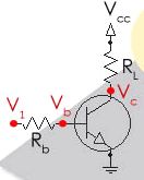
The figure shows the inclusion of an NPN transistor as a switch. You will encounter this inclusion very often when analyzing various electronic circuits. We will study how to run a transistor in the selected mode, calculate the base resistor, transistor current gain and load resistance. I suggest the simplest and most exact way for this.
1. Assume that the transistor is in saturation mode: At the same time mathematical model transistor becomes very simple, and we know the voltage at point V c. We will find the value of the base resistor at which everything will be correct.
2. Determination of collector saturation current: The voltage between collector and emitter (V ce) is taken from the transistor documentation. The emitter is connected to GND, respectively V ce = V c - 0 = V c. Once we know this value, we can calculate the collector saturation current using the formula:
Sometimes, the load resistance R L is unknown or cannot be as precise as the relay coil resistance; In this case, it is enough to know the current required to start the relay.
Make sure that the load current does not exceed the maximum collector current of the transistor.
3. Calculation of the required base current: Knowing the collector current, you can calculate the minimum required base current to achieve that collector current using the following formula:
It follows from it that:
4. Exceeding permissible values: After you have calculated the base current, and if it turns out to be lower than that specified in the documentation, then you can overload the transistor by multiplying the calculated base current, for example, by 10 times. Thus, the transistor switch will be much more stable. In other words, the transistor's performance will decrease if the load increases. Be careful not to exceed the maximum base current stated in the documentation.
5. Calculation of the required value of R b: Considering an overload of 10 times, the resistance R b can be calculated using the following formula:
where V 1 is the transistor control voltage (see Figure 2.a)
But if the emitter is connected to ground, and the base-emitter voltage is known (about 0.7V for most transistors), and assuming that V 1 = 5V, the formula can be simplified to the following: ![]()
It can be seen that the base current is multiplied by 10 taking into account the overload.
When the value of Rb is known, the transistor is "set" to operate as a switch, also called "saturation and cutoff mode", where "saturation" is when the transistor is fully open and conducting current, and "cutting" is when it is closed and not conducting current .
Note: When we say , we are not saying that the collector current must be equal to . This simply means that the transistor's collector current can rise to this level. The current will follow Ohm's laws, just like any electrical current.
Load calculation
When we considered that the transistor was in saturation mode, we assumed that some of its parameters did not change. This is not entirely true. In fact, these parameters were changed mainly by increasing the collector current, and therefore it is safer for overload. The documentation indicates a change in transistor parameters during overload. For example, the table in Figure 2.B shows two parameters that change significantly:
H FE (β) varies with collector current and voltage V CEsat. But V CEsat itself changes depending on the collector and base current, as shown in the table below.

The calculation can be very complex, since all the parameters are closely and complexly interrelated, so it is better to take the worst values. Those. the smallest H FE, the largest V CEsat and V CEsat.
Typical application of a transistor switch

In modern electronics, a transistor switch is used to control electromagnetic relays, which consume up to 200 mA. If you want to control a relay with a logic chip or microcontroller, then a transistor is indispensable. In Figure 3.A, the resistance of the base resistor is calculated depending on the current required by the relay. Diode D1 protects the transistor from the pulses that the coil generates when turned off.
2. Connecting an open collector transistor:

Many devices, such as the 8051 family of microcontrollers, have open-collector ports. The base resistor resistance of the external transistor is calculated as described in this article. Note that the ports can be more complex, and often use FETs instead of bipolar ones and are called open drain outputs, but everything remains exactly the same as in Figure 3.B
3. Creating a logical element OR-NOT (NOR):

Sometimes you need to use a single gate in a circuit and you don't want to use a 14-pin 4-gate chip either due to cost or board space. It can be replaced with a pair of transistors. Note that frequency characteristics such elements depend on the characteristics and type of transistors, but usually below 100 kHz. Reducing the output resistance (Ro) will increase power consumption but increase the output current.
You need to find a compromise between these parameters.
The figure above shows a NOR gate built using 2 2N2222 transistors. This can be done on PNP transistors 2N2907, with minor changes. You just have to consider that everything electric currents then flow in the opposite direction.
Finding errors in transistor circuits
When a problem occurs in circuits containing many transistors, it can be quite difficult to know which one is bad, especially when they are all soldered in. I give you some tips that will help you find the problem in such a scheme quickly:
1. Temperature: If the transistor gets very hot, there is probably a problem somewhere. It is not necessary that the problem is a hot transistor. Usually the defective transistor does not even heat up. This temperature increase may be caused by another transistor connected to it.
2. Measuring V CE of transistors: If they are all the same type and all work, then they should have approximately the same VCE. Search for transistors having different V CE is quick way detection of defective transistors.
3. Measuring the voltage across the base resistor: The voltage across the base resistor is quite important (if the transistor is turned on). For 5V control device NPN transistor, the voltage drop across the resistor should be more than 3V. If there is no voltage drop across the resistor, then either the transistor or the transistor control device is defective. In both cases, the base current is 0.
At one time, transistors replaced electronic tubes. This is due to the fact that they have smaller dimensions, high reliability and lower production costs. Now, bipolar transistorsare the basic elements in all amplification circuits.
It is a semiconductor element having a three-layer structure, which forms two electron-hole junctions. Therefore, the transistor can be represented as two back-to-back diodes. Depending on what will be the main charge carriers, they distinguish p-n-p And n-p-n transistors.

Base– a semiconductor layer, which is the basis of the transistor design.
Emitter called a semiconductor layer whose function is to inject charge carriers into the base layer.
Collector called a semiconductor layer, the function of which is to collect charge carriers passing through the base layer.
Typically, the emitter contains much more main charges than the base. This is the main condition for the operation of the transistor, because in this case, when the emitter junction is forward biased, the current will be determined by the main carriers of the emitter. The emitter will be able to perform its main function - injecting carriers into the base layer. They usually try to make the emitter reverse current as small as possible. An increase in emitter majority carriers is achieved using a high dopant concentration.
Make the base as thin as possible. This is due to the lifetime of the charges. The charge carriers must cross the base and recombine as little as possible with the main base carriers in order to reach the collector.
In order for the collector to be able to more fully collect media passing through the base, they try to make it wider.
Transistor operating principle
Let's look at example p-n-p transistor.

In the absence of external voltages, a potential difference is established between the layers. Potential barriers are installed at crossings. Moreover, if the number of holes in the emitter and collector is the same, then the potential barriers will be the same width.
In order for the transistor to work correctly, the emitter junction must be forward biased and the collector junction must be reverse biased.. This will correspond to the active mode of operation of the transistor. In order to make such a connection, two sources are needed. A source with voltage Ue is connected with the positive pole to the emitter, and the negative pole to the base. A source with voltage Uк is connected with the negative pole to the collector, and the positive pole to the base. Moreover, Ue< Uк.

Under the influence of voltage Ue, the emitter junction is biased in the forward direction. As is known, when the electron-hole transition is forward biased, the external field is directed opposite to the transition field and therefore reduces it. The majority carriers begin to pass through the transition; in the emitter there are 1-5 holes, and in the base there are 7-8 electrons. And since the number of holes in the emitter is greater than the number of electrons in the base, the emitter current is mainly due to them.
The emitter current is the sum of the hole component of the emitter current and the electronic component of the base.
![]()
Since only the hole component is useful, they try to make the electronic component as small as possible. Qualitative characteristics emitter junction is injection ratio.
They try to bring the injection coefficient closer to 1.
Holes 1-5 that have passed into the base accumulate at the boundary of the emitter junction. Thus, a high concentration of holes is created near the emitter and a low concentration near the collector junction, as a result of which the diffusion movement of holes from the emitter to the collector junction begins. But near the collector junction, the hole concentration remains zero, because as soon as the holes reach the junction, they are accelerated by its internal field and are extracted (pulled) into the collector. Electrons are repelled by this field.
While the holes cross the base layer, they recombine with the electrons located there, for example, like hole 5 and electron 6. And since holes come constantly, they create an excess positive charge, therefore, electrons must also come in, which are drawn through the base terminal and form a base current Ibr. This important condition transistor operation – the concentration of holes in the base should be approximately equal to the concentration of electrons. In other words The electrical neutrality of the base must be ensured.
The number of holes reaching the collector is less than the number of holes leaving the emitter by the amount of recombined holes in the base. That is, The collector current differs from the emitter current by the amount of the base current.
![]()
From here it appears transfer coefficient carriers, which they also try to bring closer to 1.
The collector current of the transistor consists of the hole component Icr and the reverse collector current.
![]()
The reverse collector current arises as a result of the reverse bias of the collector junction, so it consists of minority carriers of hole 9 and electron 10. Precisely because the reverse current is formed by minority carriers, it depends only on the thermal generation process, that is, on temperature. Therefore it is often called thermal current.
The quality of the transistor depends on the magnitude of the thermal current; the smaller it is, the better the transistor.
The collector current is connected to the emitter current transfer coefficient.
The currents in the transistor can be represented as follows